
 |
| Six-core Opteron Microprocessor die |
A microprocessor is an integrated circuit built by hundreds of millions of transistors. It is the brain of any computer and is in charge of executing every program in it. Such programs can be the operating system, the device drivers or even the simplest application software.
The operation of a microprocesor is based on the execution of simple logic-arithmetic instructions such as addition, substraction, mutiply, divide, and, or, not, etc. The rest of the fundamental instructions are data transfer and memory acces operations.
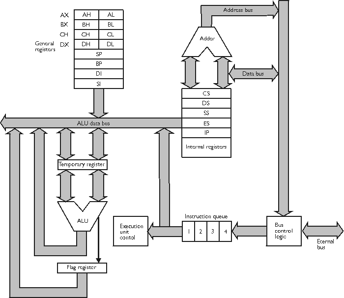
The figure below shows the 8088 CPU block diagram. The 8088 was one of the popular microprocessors in computers history and was released by intel in 1979. Such a basic microprocessor consisted of an arithmetic-logic unit (ALU), control registers, general purpose registers, the data bus, and the address bus. Modern microprocessors are much more complex and include features such as pipelining, out of order execution, and floating point units.
The operation of a microprocesor is based on the execution of simple logic-arithmetic instructions such as addition, substraction, mutiply, divide, and, or, not, etc. The rest of the fundamental instructions are data transfer and memory acces operations.
The figure below shows the 8088 CPU block diagram. The 8088 was one of the popular microprocessors in computers history and was released by intel in 1979. Such a basic microprocessor consisted of an arithmetic-logic unit (ALU), control registers, general purpose registers, the data bus, and the address bus. Modern microprocessors are much more complex and include features such as pipelining, out of order execution, and floating point units.
Now that we know a little about the structure of a basic microprocessor, let us explore in more detail each one of its parts.
In the first place we find the control unit, which is the functional block in charge of sinchonizing all the operations in a CPU. The specific functions this unit accomplishes are: instruction fetching, controlling the data transfer between the main memory and the registers, and controlling the ALU operation.
In second place we have the registers, and we can find basically two types of them. The first type are the specific purpose registers (SPRs) and the second type are the general purpose registers (GPRs).
The SPRs allow to have a record of the procesor status. Some of the most important are the program counter (PC), the flag status registers and the stack pointer (SP). The program counter always points to the program memory address of the instruction that is in execution, and its value is incremented by 1 each cycle, except when a branch or jump instruction is executed. In sumary, the PC determines the flow of execution of the instructions that are stored in program memory. The flag status register, as its name suggest, stores the status of the different flags that are set or reset by specific events, such as arihtmetic-logic operations, interruptions, and registers overflow. The most important status flags in a CPU are: The Sign Flag (SF), Zero Flag (ZF), Carry Flag (CF), Overflow Flag, and Interrupt Flag (IF). The stack pointer stores the most recent address used in the stack. The stack is a reserved space in main memory used to save the processor status when calling subroutines or when the program runs out of GPRs.
On the other hand, the general purpose registers are the ones in charge of temporarily storing the operands for instructions, as well as their results. Additionally, GPRs can be also used as main memory pointers. Early processors had limited number of GPRs, this limitation posed an important issue because when the CPU ran out of registers or had a subroutine call, the program was forced to use the stack. The problem with the stack is that it stores data in main memory which is slower, in orders of magnitude, than accesing the internal registers. Using the stack represented a really huge impact in performance. Additionaly, with the introduction of out of order superscalar processors, other problems arised due to the lack of GPRs. The data hazards produced by the execution of multiple instructions per cycle, posed an important drawback that limited the potential performance of superscalar CPUs. In order to avoid the problems associated with the lack of registers, modern processors include arrays with a huge number of non-architectural registers, known as register file. By using a register file a CPU can use techniques such as register renaming and register window to overcome the aforementioned issues.
The third block we find is the Arithmetic-Logic Unit (ALU). As it was mentioned at the beggining of this article, this unit is in charge, as its name suggest, of performing basic arithmetic and logic operations.
The fourth component is the data bus, which allows the CPU to comunicate with he external world. Through this bus all the data to be processed is received and the obtained results are sent out.
And last but not least, there is the address bus, which is in charge of addresing the external physical memory. The witdh of this bus determines how much memory the processor is able to address. For example, if the processor has a 32 bit address bus, it will be able to address up to 4 GBs of RAM.
Another important block that is included in modern microprocessors is a floating point unit (FPU). A FPU is a special mathematical processing block that enables the processor to produce more precise arithmetical results when performing operations on non-integer numbers. Processors released previously to the intel 486 did not include a FPU and required an external mathematical co-processor in order to execute such instructions.
In this article we have explored the basics of a microprocessor, its structure, its functional blocks and their specific functions. We will be posting even more detailed articles about the operation of modern microprocessors, their issues, their functional blocks, etc.
0 comments:
Speak up your mind
Tell us what you're thinking... !